Single quantum dot absorption nanospectroscopy
We have observed, at room temperature,
the ultrasmall absorption, as small as 10-9, of a single buried
semiconductor quantum dot in the mid-infrared. The observation
around λ~10 µm wavelength with a spatial ~ 60 nm resolution (i.e.
~λ/150) is achieved by coupling an atomic force microscope based
detection with a mid-infrared pulsed laser excitation. This
"nanospectroscopy" is applicable to a large variety of single buried
solid-state and biological nano-objects and offers new perspectives to
optically address, monitor and manipulate individually semiconductor
quantum dots for quantum information processing and cavity quantum
electrodynamic measurements.
This work was performed in collaboration with the free-electron laser team (CLIO - Laboratoire de Chime Physique CNRS-Univ. Paris Sud) and the epitaxy group of Laboratoire de Photonique et Nanostructures (LPN-CNRS).
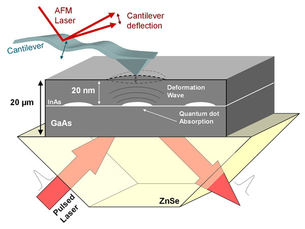
A schematic description of the photoacoustic setup is depicted in Fig. 1. The set-up is based on a photothermal measurement using an atomic force microscope in the mid-infrared (AFMIR) recently developed at the free-electron laser facility CLIO. The n-doped InAs/GaAs self-assembled quantum dots were grown by molecular beam epitaxy with a 400 µm-2 sheet density (average dot distance of 50 nm). The doped quantum dots, buried 20 nm below the surface, are excited at room temperature by the infrared picosecond pulses of a free-electron laser. The energy absorbed by a single quantum dot is expected to be non-radiatively transferred to the lattice by the emission of optical phonons and their anharmonic decay into acoustical phonons. The local thermal expansion generates a deformation field and launches a displacement impulse that propagates in a few ps towards the surface (Schematic illustration in Fig. 2). The local surface displacement is probed by the gold-covered tip of an atomic force microscope operated in contact mode. The atomic force microscope (AFM) tip contact surface sets the lateral resolution down to the nanometer scale (tip radius is 200 nm, contact radius is ~2 nm). The strain pulses induce a percussional excitation of the AFM cantilever on a ps time scale, i.e. on a much smaller time scale than bulk heat diffusion. The energy provided by the picosecond pulse excitation is finally transferred to the low frequency vibration modes of the cantilever. The free-electron laser delivers pulse sequences (8 µs length duration) at a repetition rate of 25 Hz, each of them containing picosecond pulses separated by 32 ns. The average incident power on the ZnSe prism is around 10 mW.
Fig. 3 presents a two-dimensional 800 x 800 nm2 image of a quantum dot sample, sample S1, for which the electron population is provided by a 4 x 1011 cm-2 density Si delta-doping layer inserted 2 nm beneath the wetting layer. The excitation wavelength is 9.6 µm. The value at each pixel of the image is obtained by integrating the signal over the vibrational modes of the cantilever (25 – 75 kHz). The pixel size is 20 nm. The white color corresponds to the mid-infrared absorption signature of single quantum dots. Only a small fraction of the quantum dots can be observed on the image among the ~250 quantum dots statistically buried under the surface since all quantum dots are not significantly populated at room temperature as a result of the balance between carrier capture and thermionic emission. Moreover only a fraction of the quantum dots exhibits an absorption spectrally resonant with the laser wavelength. The typical effective quantum dot size revealed by this measurement is 3-4 pixels, i.e. 60 - 80 nm. The larger spots are attributed to a gathered group of several dots which can not be spatially resolved.
This work was performed in collaboration with the free-electron laser team (CLIO - Laboratoire de Chime Physique CNRS-Univ. Paris Sud) and the epitaxy group of Laboratoire de Photonique et Nanostructures (LPN-CNRS).
A schematic description of the photoacoustic setup is depicted in Fig. 1. The set-up is based on a photothermal measurement using an atomic force microscope in the mid-infrared (AFMIR) recently developed at the free-electron laser facility CLIO. The n-doped InAs/GaAs self-assembled quantum dots were grown by molecular beam epitaxy with a 400 µm-2 sheet density (average dot distance of 50 nm). The doped quantum dots, buried 20 nm below the surface, are excited at room temperature by the infrared picosecond pulses of a free-electron laser. The energy absorbed by a single quantum dot is expected to be non-radiatively transferred to the lattice by the emission of optical phonons and their anharmonic decay into acoustical phonons. The local thermal expansion generates a deformation field and launches a displacement impulse that propagates in a few ps towards the surface (Schematic illustration in Fig. 2). The local surface displacement is probed by the gold-covered tip of an atomic force microscope operated in contact mode. The atomic force microscope (AFM) tip contact surface sets the lateral resolution down to the nanometer scale (tip radius is 200 nm, contact radius is ~2 nm). The strain pulses induce a percussional excitation of the AFM cantilever on a ps time scale, i.e. on a much smaller time scale than bulk heat diffusion. The energy provided by the picosecond pulse excitation is finally transferred to the low frequency vibration modes of the cantilever. The free-electron laser delivers pulse sequences (8 µs length duration) at a repetition rate of 25 Hz, each of them containing picosecond pulses separated by 32 ns. The average incident power on the ZnSe prism is around 10 mW.
 |
 |
|
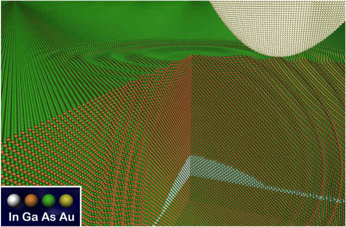
| Fig. 1 : Schematic description of the AFM experimental set-up and operation principle for the room temperature measurement of the ultraweak absorption. | Figure 2 : Artistic illustration of the local matrix deformation generated by the quantum dot absorption. The virtual deformation is represented as a spherical acoustic wave packet. In pratice it corresponds also to a thermal matrix dilation. The buried quantum dot appears in white color. The image also represents the AFM tip on the surface. |
Fig. 3 presents a two-dimensional 800 x 800 nm2 image of a quantum dot sample, sample S1, for which the electron population is provided by a 4 x 1011 cm-2 density Si delta-doping layer inserted 2 nm beneath the wetting layer. The excitation wavelength is 9.6 µm. The value at each pixel of the image is obtained by integrating the signal over the vibrational modes of the cantilever (25 – 75 kHz). The pixel size is 20 nm. The white color corresponds to the mid-infrared absorption signature of single quantum dots. Only a small fraction of the quantum dots can be observed on the image among the ~250 quantum dots statistically buried under the surface since all quantum dots are not significantly populated at room temperature as a result of the balance between carrier capture and thermionic emission. Moreover only a fraction of the quantum dots exhibits an absorption spectrally resonant with the laser wavelength. The typical effective quantum dot size revealed by this measurement is 3-4 pixels, i.e. 60 - 80 nm. The larger spots are attributed to a gathered group of several dots which can not be spatially resolved.
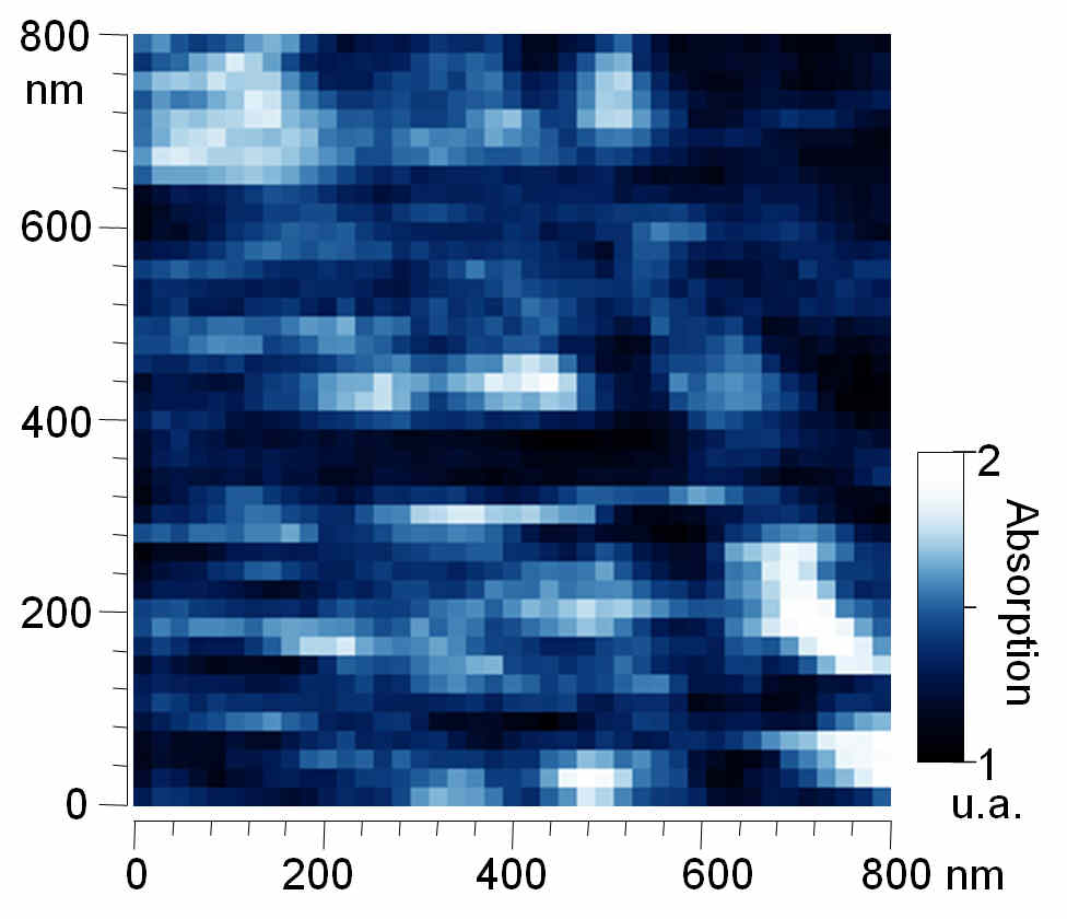 |
| Figure 3
: Absorption of buried quantum dots (white contrast) at an
excitation wavelength λ=10 µm. The spatial resolution is 60
nm, i.e. approximately λ/150 |
A general French article:
"Microscopie moyen infrarouge de nano-objets individuels"
S. Sauvage, P. Boucaud, A. Dazzi, J.-M. Ortéga
Image de la physique, 80, CNRS (2009).
pdf.