Quantum dot modeling
Quantum dot geometry and composition
Strain field
Three-dimensional 8 band k.p resolution of the Schrödinger equation
Resolution
Simple view of the electronic structure
A more sophisticated view
The theoretical knowledge of the electronic structure of III-V self-assembled quantum dots is a crucial step towards the interpretation and the understanding of the infrared experimental data. The knowledge of the electronic structure is naturally a precious basis for the spectroscopy but also brings valuable theoretical information that cannot be directly accessed experimentally. Because of the three-dimensional confinement, the density of states is delta-like with well energy separated energy levels, instead of being composed of continuous bands or sub-bands of energy levels as it is the case in quantum wells or bulk semiconductors. Depending on the size and geometry, numerous levels can be confined in the conduction band and even more in the valence band. Non intuitive selection rules, dipole lengths or polarizations can rule the optical transitions between these levels. In the case of two-dimensional heterostructures, a relevant electronic structure can be obtained at a very low computational cost in rather simple single band parabolic envelope function models. As opposed to quantum wells and for many reasons the calculation of the energies of the confined levels, wave functions, and dipole matrix elements in quantum dots is a challenging issue.
On the one hand an exhaustive calculation of the electronic structure should first take into account the specific geometry of the dots and specifically the confinement along the three directions of space, even if the lateral dimensions are ten times longer than along the growth axis. The lack of spatial symmetry in the geometries of the quantum dots usually implies high cost three-dimensional computations. This can be the case for quantum dots with an elongated geometry that presents no continuous nor discrete symmetries. Several electronic bands must be considered because of the large confinement energies. The confinement energies can be 10 times that of quantum wells because the strong confinement of the carriers along the growth axis and in the layer plane. Non-parabolicity of band diagram of underlying semiconductors used to construct the heterostructure is thus no longer negligible. It results in a correction in the energies of about 30% as compared to what can be expected from a parabolic dispersion and leads to strong band mixing. The electronic structure also depends on the strain field which is present in these lattice-mismatched materials. The strain can be inhomogeneous within the dot, involving not only biaxial components but also non negligible shear components. The surrounding of the dot is also strained and can play a significant role on the bound-to-continuum transitions. The effect of strain on core and barrier material band structures should be considered since it modifies the energy band gaps and lifts up the heavy-light hole degeneracy at the zone center. The piezoelectric field originating from the shear component of the strain should also be taken into account since it changes the level energies. There is also an inhomogeneous broadening of the optical properties of dot ensembles due to the size fluctuation from dots to dots and from one dot plane to another and thus there is the necessity to consider dot of different sizes, shapes and compositions. Coulomb interactions finally can play a non negligible role in multi-charged quantum dots.
On the other hand a difficulty comes from a relative uncertainty on the input parameters. Despite numerous experimental characterizations, the exact geometry, the composition, the effect of the In segregation are not perfectly known experimentally. These parameters will depend on the growth conditions and a slight variation on their values (e.g. composition) can lead to strong deviations on the calculated electronic structures (e.g. interband transition energies).
Several theories have been developed to assess the electronic structure of the quantum dots. The simplest and first developed approach is based on the effective-mass theory. Single-band effective-mass calculations have been performed for InAs/GaAs dots with various geometries: cones, square based pyramids , thick lenses, flat lenses. Note that a simple cubic quantum box model gives very crude predictions on the dipole matrix elements and level energies as compared to those provided by a 3D model which accounts for the realistic geometry of the dots. 3D single band effective mass is often a good compromise if one does not require accurate energy predictions. Otherwise k.p calculations including 4, 6 and 8 bands have also been performed on square based pyramids or flat lens shapes . These multiband calculations account for the band-mixing and in particular for the non-parabolicity. Note that microscopic semiempirical pseudopotential methods are limited in the same way as k.p techniques because of the present lack of accuracy on the input parameters.
Quantum dot geometry and composition
The InAs quantum dots are grown by molecular epitaxy on [001] GaAs substrate. From structural measurements the dot density is around 4x1010 cm-2. In the literature, various geometries for InAs islands grown on GaAs have been reported: thick or flat lenses, square-based or elongated pyramids with different facet orientations. These geometries mainly depend on the growth conditions. Here the geometry is chosen according to both transmission electron microscopy (TEM) and cross-section scanning tunnelling microscopy (XSTM) structural characterizations. These studies show that the InAs dots grown on GaAs that we have investigated roughly have a lens-shaped geometry with a low aspect ratio of ~ 0.1 (height over diameter) as seen in Figure 1. Typical heights span the 1.5-2.5 nanometer range. From XSTM the dot core is found to be constituted of pure InAs with a sharp interface between InAs and the GaAs barrier with a roughness below 0.5 nm. In the calculation, the InAs volume is thus modelled as follows: a portion of a sphere, 2.5 nm high and 25 nm in diameter, lying on the bottom of a 0.5 nm thick wetting layer.
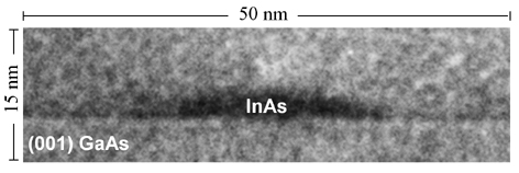 |
| Figure 1 : Cross section image of an InAs
quantum dot imbedded into a GaAs matrix obtained by Transmission
Electron Microscopy (Courtesy of Gilles Patriarche, Laboratoire de
Photonique et Nanostructures, CNRS, Marcoussis). |
Strain field
Self-assembled quantum dots are strained heterostructures since their Stranski-Krastanow growth mode uses the natural lattice mismatch between the substrate and the deposited material. In the case of the InAs/GaAs couple, this mismatch is around 7% and leads to a strong strain field within and around each quantum dot. The 3D components eij of the strain tensor are key parameters on which depends the electronic structure of the bulk underlying materials (InAs and GaAs for the system presented in this article) and thus the electronic structure of the quantum dot. The band gap of InAs is increased by more than 100 meV due to a 7% in-plane applied strain as compared to unstrained InAs. The heavy-light hole degeneracy at the zone center is also strongly lifted pushing the light hole band around 200 meV beneath the heavy hole band. As compared to quantum wells one a priori expects the presence of non-vanishing 3D shear components because of the 3D nature of the quantum dot geometry. This component is at the origin of a piezoelectric field that can be non negligible, especially in the case of high aspect ratio islands.
The strain field can be calculated by minimizing the strain energy Estrain given by a valence force field theory :
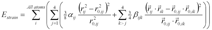 (1)
(1)In this microscopic theory the strain energy is expressed from the variation of the bond length and bond angles for all the atoms within the deformed zinc-blend lattice. In equation (1) is the vector going from atom i to atom j, the vector from atom i to atom k in the unstrained crystal, the indexes j and k designing one of the four nearest neighbour of atom i. Taking into account the strain limit conditions set by the substrate, the minimization gives access directly to the displacement of the atoms at an interatomic length scale, in particular around the hetero-interfaces, respecting the 43m symmetry of the crystal and depending solely on the chosen dot geometry and local dot and barrier compositions. One will note that, for each material InAs or GaAs, there are only two input coefficients (bond stretching alphaij and bond-angle bending betaijk) to generate the macroscopic elastic properties given by three independent elastic constants. In practice for InAs/GaAs the main two lattice constants (C11, C12) are fitted exactly at the expense of the third less important one (C44) fitted with an acceptable 10% error. C44 is involved in the shear component of strain and plays a lesser role for flat geometries.
Fig. 2 depicts a representation of the strain field of one flat lens-shaped pure InAs self-assembled quantum dot floating over a 0.5 nm thick InAs wetting layer and inserted into a zinc-blend GaAs matrix. For a height of 2.5 nm and a base diameter of 25 nm the calculation shows that the volume dilation is essentially localized into the InAs volume while the GaAs barriers remain nearly unstrained. A more detailed analysis shows that the strain tensor is close to the one of a thin InAs quantum well grown on GaAs: the relative elongations are nearly piecewise constant (i.e. nearly constant in the InAs volume and nearly constant in the GaAs volume) and the shear component in only moderate near the interfaces. The main reason for this specificity is the small aspect ratio (0.1) of the dot. One also expects much smaller piezoelectric field in this flat dot than for high aspect ratio geometry. In quantum dots exhibiting a higher aspect ratio, the piezoelectric potential may lead to significant corrections (~ 10 meV) to the level energies. In what follows we will consider that the strain field is biaxial piecewise constant and we will neglect the effect of piezoelectricity on the level energies.
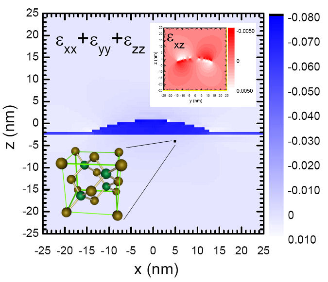 |
| Figure 2 : Compressive and shear components of
the strain field in an InAs/GaAs self-assembled quantum dot calculated
by minimizing the strain energy given by a microscopic valence force
field theory. The
compressive component (blue) is roughly piecewise constant and located
into
the InAs volume and mimics the strain of a thin InAs quantum well. The
non
negligible shear component corresponds (red) to less than 3% of lattice
deformation. |
Three-dimensional 8 band k.p resolution of the Schrödinger equation
The theoretical electronic structure of one quantum dot, i.e. the confined level energies and wave functions, is provided by the three-dimensional resolution of the Schrödinger equation (2) written in a 8 band k.p formalism taking into account a realistic flat-lens shaped geometry for the quantum dot. The base of the InAs lens is deliberately 10% elongated along the [110] direction to account for spectroscopic data. The Pidgeon-Brown Schrödinger equation is written :
where Hkp8, Hstrain, V, and E are the unstrained 8 band k.pHamiltonian matrix containing 168 real in-space acting operators, the strain Hamiltonian, the confining potential, the envelope wave function of the eigenstate and the energy respectively. The 8 bands include the conduction band, the heavy hole, light hole and spin-orbit split-off bands with a quantized spin along the growth axis. This formalism is a well-known and powerful mean to describe accurately the band structure of bulk semiconductors near the zone center. It is used here along with the envelope function theory to extract a realistic description of the nanostructure states. The 8 band k.p matrix operator takes into account the valence band mixing, valence-conduction band coupling at the origin of the non-parabolicity of the dispersion relation and strain effects. The strain field is biaxial with an in-plane deformation imposed by unstrained GaAs barriers. The resolution of the Schrödinger equation gives access to the confined level energies E and 3D envelope wave functions from which all the matrix elements are extracted. For the infrared data analysis, we consider specifically intersublevel transitions between either conduction states or valence states. The dipole lengths as well as the polarization of the transitions (in the layer plane, along the growth axis) are key parameters with the transition energies that enable to disentangle the infrared experimental data.
Resolution
The 8 band k.p 3D Schrödinger equation is solved numerically by finite difference or finite element discretization on a typically 70x70x50 uniform parallelepiped cell grid. The dot and the wetting layer volumes are encompassed into a large infinite wall box (40x40x30 nm3) in order to limit the size of the discretized Hamiltonian and to impose null or periodic wave function conditions at the edge of the box. The confining box is chosen large enough so that the energy of the states confined within the dot remains nearly unaffected by a change of the box dimension. The resulting finite rank Hamiltonian matrix is then partially diagonalized using a customized iterative block Jacobi-Davidson algorithm implemented in Javel, the C++ Schrödinger computation program compiled on a 1 GHz processor Personal Computer. The program is stopped when the vector residual normalized by the eigenenergy reaches a lower enough threshold of 10-6. The algorithm allows the determination of up to 100 first confined state energies and their associated wave functions from which are extracted the dipole matrix elements (length, polarization) and Coulomb interaction energies of the intersublevel transitions.
Note that from a mathematical and numerical point of view the resolution of the Schrödinger equation is not straightforward. As far as finite difference is concerned, there are well known and systematic methods applied for parabolic or elliptic differential equations. Unfortunately the 8 band k.p Schrödinger equation is hyperbolic and such systematic approach is not available. The simultaneous search for consistence and numerical stability of the discretization schemes can be very tedious. Even when the mathematics of the discretization schemes is clear, there are still numerical issues related to the diagonalization of the large rank (106 to 107) matrix, choice of preconditionners and efficient extraction of eigenvalues and eigenvectors interior to the matrix spectrum.
Simple view of the electronic structure
It is instructive to first consider the electronic structure given by a cubic quantum box with infinite barrier heights. In this case, the electronic structure results from the independent combination of the states of infinite wall quantum wells of respective widths Lx, Ly, Lz along the three x, y and z directions. If the carrier lives in a parabolic single band described by the scalar effective mass matrix (mxx, myy, mzz) then the level energies have the simple following form:
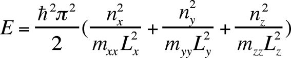 (3)
(3)and the envelope wave functions the form:
where nx, ny, nz are positive non null integers. One interest of this simple model is to show that the states can be sorted by the numbers of the wave function nodes nx, ny, nz along the three directions of space. According to this notation, the ground state is labelled 000, the first excited state resulting from the confinement along the x-axis is 100 and so on. Allowed optical intersublevel transitions between level i and j only exist between states of odd difference quantum numbers along the same axe, e.g. 000->100, 100->200, 000->300 but not 000->200, 100->001 etc. In a non-cubic quantum box, a convention is to label the states from the denomination they would have in the cubic dot obtained by continuously deforming the original dot.
A more sophisticated view
Figure 3 depicts the electronic structure of one InAs/GaAs self-assembled quantum dot as deduced from the 3D resolution of the 8 band k.p Schrödinger equation. Note that this picture forms a base from which polaronic structure (discussed in the next section) can be understood. In what follows we will forget the spin since all the states are doubly spin degenerated. The ground state is located around 300 meV above the InAs band edge as a result of the strong confinement along the three directions of space. The confinement comes essentially from the growth axis. The envelope wave function is s-like so this state is called the s state instead of e000. Note that because of the strong confinement energy this conduction state is constructed using the non-parabolic part of the band structure of InAs and GaAs and that 10% of the square envelope function is projected onto the valence basis. The wave functions of the first two electronic excited states are p-like and thus are referred to as the “p” states instead of e100/e010. The splitting between the p states originates from the elongated geometry and the slightly stronger confinement along [110] than along [110] crystal direction. The s-p transition is predicted at 56 and 63 meV corresponding to wavelengths around 20 µm. The s-p transition is a model of intersublevel transitions in semiconductor quantum dots. It is well isolated from other transitions, it occurs between well confined levels far from the continua, it has a large oscillator strength with a predicted dipole length as long as 3.4 nm and is fully polarized in the layer plane. At higher energy the energy spectrum contains 3 highly excited discrete states, called the “d” states (corresponding in a cylindrical symmetry quantum dot to two "1d" and one "2s" states). The other calculated states lie above the wetting layer energy and their wave functions appear to be delocalized. As a matter of fact these states are the first ones of a set of states either delocalized in the wetting layer (subband-like states) or three-dimensionally delocalized around the dot (bulk-like states). They belong to what will be respectively called in the following the continuum of the wetting layer and the continuum of the GaAs barriers. Naturally these states, which strongly depend on the choice of the large confining box used to solve the equation, become even better approximations of the states of the continuum when the size of the large box increases towards infinity. The onset of the wetting layer continuum, i.e. the energy of the first states starting to delocalize into the wetting layer, is around 30 meV below the GaAs band edge or equivalently 120 meV above the ground state. Note that as far as the conduction states are concerned, no level e001 corresponding to the confinement along the growth axis is predicted to be confined. This is confirmed experimentally, the main reason being the too strong confinement along the growth axis (the height of the quantum dot is 2.5 nm).
In the valence band, despite the smaller barrier height a much larger number of states are confined because of the heavier effective masses. Only the very first states are represented in Figure 3. The confinement energy of the ground state h000 is also smaller than in the conduction band. From a general point of view, the valence electronic structure is more complex than the conduction one.
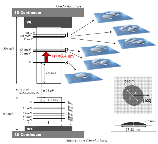 |
| Figure 3 : Electronic structure of a InAs/GaAs
self-assembled quantum dot as deduced from the 3D resolution of the
Schrödinger equation written in a 8 band k.p formalism. The
resolution takes in account a realistic elliptical flat lens-shape
geometry (25x28x2.5 nm3) described in the inset. The
representation of the envelope wave functions considers probability
volumes including 2/3 of the presence probability of the electron. WL
denotes
the wetting layer 2D continuum, beneath the bulk barrier 3D continuum. |