Reasearch in the quantum dot & photonic nanostructures group
NB: this page is outdated
 |
Optical spectroscopy
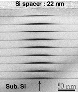
of nanostructures Optical spectroscopy is a powerful tool to analyze the electronic structure of self-assembled quantum dots. The optical recombination between conduction states and valences states can be probed by photoluminescence or photoluminescence excitation. Absorption or emission measurements in the mid-infrared or far infrared spectral ranges in doped nanostructures can bring valuable information on intersublevel transitions. The information obtained by optical spectroscopy are compared with the calculated electronic structure of the islands. Both InAs/GaAs and Ge/Si self-assembled islands are investigated. |
 |
Modeling of the
electronic structure of nanostructures The knowledge of the energy of the confined states and their wavefunctions is a key parameter to understand the physics of the nanostructures. Several numerical codes have been developed. The electronic structure of InAs/GaAs quantum dots is calculated by solving the 3D Schrödinger equation in a 8 band k.p formalism. The strain field in and around the islands is calculated with a microscopic valence force field model. Quantum well-like calculations have been developed for strained SiGe/Si heterostuctures with a 6 band or 14-band k.p formalism |
| Single
quantum dot absorption nanospectroscopy Buried single quantum dots can be locally observed through their luminesence properties. The observation of quantum dots through their absorption is far more difficult and becomes very challenging for intersublevel quantum dot absorption in the mid-infrared. At room temperature, the transmission variation due to the intersublevel absorption of a single quantum dot is as low as 10^-9 using a diffraction-limited set-up for a 10 µm wavelength excitation. The spatial resolution is in the latter case limited to half the wavelength. We have develeoped a novel technique to image the ultra-weak absorption of buried single quantum dots. This technique combines a picosecond optical excitation and the local absorption measurement through the vibrations of an atomic force microscope cantilever positioned in contact mode above the quantum dot. The spatial resolution of the measurement is around 60 nm, well beyond the diffraction limit. |
 |
Photonic devices :
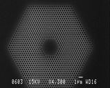
semiconductor quantum dots and photonic crystals Photonic crystals are obtained by periodically modulating the permittivity of materials. Photonic band gaps for which light propagation is inhibited can thus be obtained, at wavelengths matching the 1.3 - 1.55 µm specral ranges. The photonic crystals modify the density of optical modes and the radiation pattern of emitters. Microcavities with high Q factor and small mode volumes can be easily obtained. These structures offer new opportunities for the development of nanophotonics with silicon-based materials. In our group, two-dimensional photonic crystals are designed and fabricated on silicon-on-insulator substrates. Ge/Si self-assembled islands emitting around 1.3 – 1.55 µm are used to probe the photonic structures. We are developing nanosources with these silicon-based materials. A microphotoluminescence set-up is used to characterize the cavities. |
 |
Quantum
information
processing with quantum dots Semiconductor quantum dots are potential candidates for quantum information processing, either as single photon sources or support for charge or spin qubits. In many quantum information schemes, the interaction of the qubits with the environment and the dephasing set the fundamental limits. The control of the interaction between qubits is a key factor to implement quantum logic gates. We study the relaxation dynamics of polarons, which are electron-phonon entangled quasiparticles, the Rabi oscillation of polarons, the dephasing mechanisms of charge excitations by four-wave mixing measurements on ensemble of quantum dots and vertically coupled quantum dots. These measurements are performed with femtosecond or picosecond optical pulses. |
