Germanium photonics
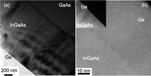 |
High quality tensile-strained n-doped germanium thin films grown on
InGaAs buffer layers by metal-organic chemical vapor deposition We
show that high quality tensile-strained n-doped germanium films can be
obtained on InGaAs buffer layers using metal-organic chemical vapor
deposition with isobutyl germane as germanium precursor. A tensile
strain up to 0.5% is achieved, simultaneously measured by x-ray
diffraction and Raman spectroscopy. The effect of tensile strain on
band gap energy is direcly observed by room temperature direct band gap
photoluminescence.
Appl. Phys. Lett. 98, 091901 (2011) http://link.aip.org/link/?APL/98/091901 |
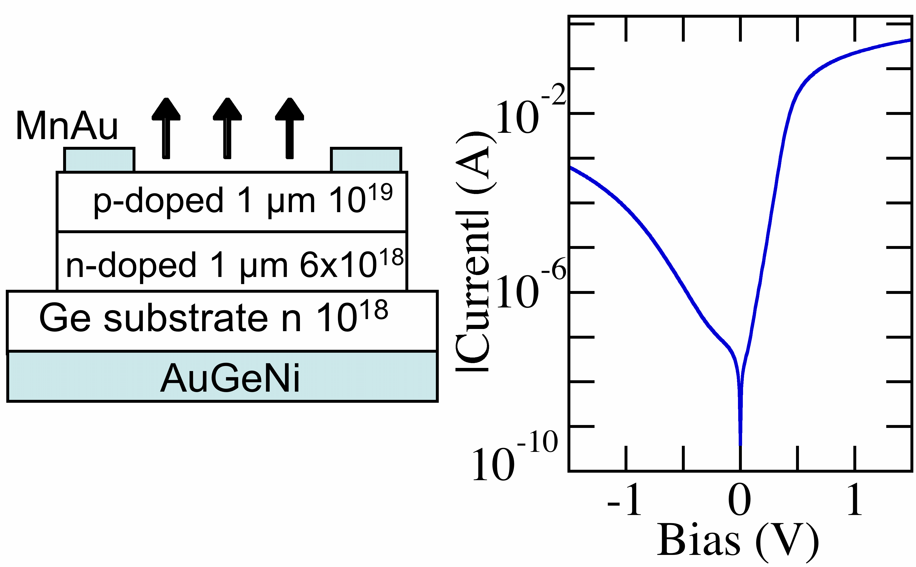 |
Direct and indirect band gap room temperature
electroluminescence of Ge diodes We
have investigated the room temperature electroluminescence of pure
germanium diodes grown by metal organic chemical vapor deposition. The
dependence of the optical response of the p-n diodes is studied as a
function of the injected current. Both direct and indirect band gap
recombinations are observed at room temperature around 1.6 and 1.8 m.
The amplitude of the direct band gap recombination is equivalent to the
one of the indirect band gap.
J. Appl. Phys. 108, 023105 (2010). http://link.aip.org/link/?JAP/108/023105 |
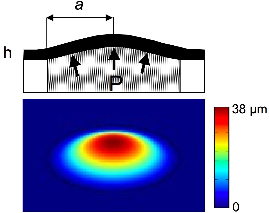 |
Control
of direct band gap emission of bulk
germanium by mechanical tensile strain We have shown that the
recombination energy of the direct band gap photoluminescence of
germanium can be controlled by an external mechanical stress. The
stress is provided by an apparatus commonly used for bulge or blister
test. An energy red-shift up to 60 meV is demonstrated for the room
temperature photoluminescence of a thin germanium membrane (125 nm
wavelength shift from 1535 to 1660 nm). This photoluminescence shift is
correlated to the in-plane tensile strain generated in the film. A
biaxial tensile strain larger than 0.6 % is achieved by this method.
This mechanical strain allows to approach the direct band gap condition
for germanium which is of tremendous importance to achieve lasing with
this material.
Appl. Phys. Lett. 96, 041909 (2010) http://link.aip.org/link/?APL/96/041909 |
 |
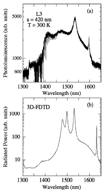 |
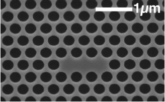
Two-dimensional photonic crystals with germanium on insulator obtained by a condensation method Germanium on insulator on
silicon substrates can be obtained by the growth of a SiGe layer on
silicon on insulator followed by a condensation at high temperature and
a Ge epitaxial growth. We have shown that these substrates can be used
for photonic devices. Two-dimensional photonic crystals with defect
cavities have been fabricated. The emission at room temperature of
condensed germanium can be spectrally controlled by varying the lattice
parameter of the photonic crystals. Resonant emission is obtained
between 1400 and 1700 nm when modifying the lattice periodicity between
400 and 480 nm for L3 cavities in a triangular lattice. Quality factors
of 540 are obtained for the fundamental mode of the L3 cavity around
1600 nm. The experimental radiation pattern of the defect cavities is
compared to the one calculated by a finite-difference time-domain
method. A specificity of the germanium-on-insulator photonic crystals
is that the optical sources are distributed within the whole material,
by opposition to photonic crystals with a single quantum dot layer
internal source.
Optics Communications 281, 846 (2008) |